Advanced Delay Modeling
Comprehensive guide to hierarchical circuits, delay modeling, timing checks, and electrical attributes.
Introduction
SIMIC supports many features that facilitate circuit description, allow accurate delay modeling and rapid detection of timing problems. This chapter describes how to represent circuits hierarchically, describe delay and loading characteristics, and create cell libraries. It also describes how SIMIC handles special circuit configurations, such as wire-ties and paralleled elements.
Design verification is often performed as a two-step process. The first step is to verify functionality, that is, making sure that the logical design is correct and complete. Addressing timing problems at this point would unnecessarily complicate the task. With this goal successfully accomplished, the second step is to detect and correct timing problems. Following this methodology requires that the user be able to control the degree of timing checks and pessimism introduced during simulation. This chapter describes how to accomplish this control from the SNL circuit description. Much of this control is also available with SIMIC run commands issued during simulation (see Circuit Troubleshooting).
Whenever a new SNL keyword is introduced in this chapter, its valid abbreviations (if any) are also given in parentheses.
Hierarchical Description
SNL supports hierarchy in a regular manner. As described in Circuit Modeling Fundamentals, each PART statement instantiates a component and connects it to other components in a type block. The components can be built-in primitives, user-defined primitives, or macros (structural descriptions of subcircuits containing primitives and/or other macros; the lowest level macros contain only primitives). The type of component is specified by the PART statement's TYPE keyword field.
In general, a SNL description contains one or more type blocks, each defining a macro or BOOLEAN subcircuit. All type blocks begin with a TYPE statement that defines the subcircuit's pins and their electrical characteristics. In a macro, PART statements follow the TYPE statement to describe its internal structure. An entire circuit description can span multiple files.
A macro’s depth, or level of nesting, is unrestricted.

.7.2.1 Instantiating Macros
A four-bit ripple-carry adder will be used as an example to illustrate hierarchical SNL descriptions. Figure 15(a) illustrates the one-bit full-adder circuit from Basic Simulation, which is used here as the basic adder cell, and Figure 15(b) illustrates the four-bit adder's block diagram. (The exclusive-or gate and its output signal, s[4], are not really part of the four-bit adder structure; this element performs sign extension of the four-bit inputs to produce the proper sign bit of a five-bit sum.)
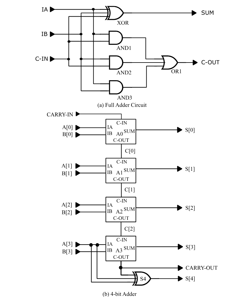
Figure 15 - Four-bit Adder Circuit
The SNL descriptions of both the full-adder and the four-bit adder are shown in Figure 16.
!format p= t= i= o=
type=full-adder i=ia,ib,c-in o=sum,c-out
xor exor ia,ib,c-in sum
and1 and ia,c-in and1
and2 and ib,c-in and2
and3 and ia,ib and3
or1 or and1,and2,and3 c-out
type=four-bit i=a[3:0],b[3:0],carry-in $
o=s[4:0],carry-out
%declare integer2 = a[3:0],b[3:0],s[4:0]
s[0],c[0] a0 full-adder a[0],b[0],carry-in
a1 full-adder a[1],b[1],c[0] s[1],c[1]
a2 full-adder a[2],b[2],c[1] s[2],c[2]
a3 full-adder a[3],b[3],c[2] s[3],carry-out
s4 exor a[3],b[3],carry-out s[4]
Figure 16: SNL Description of a Hierarchical Four-Bit Adder
The first point to note is that the PART statements instantiating the full-adders are structurally no different from the PART statements that instantiate primitives. The second point is that the number of inputs and outputs of each instantiated full-adder agrees with the number of inputs and outputs of the full-adder macro, since there is a one-to-one correspondence. For example, part a1 in the four-bit macro has three inputs, a[1],b[1],c[0] that are connected to pins a,b,carry-in, respectively, of the instantiated full-adder macro, and two outputs, s[1],c[1], that are connected to the macro’s output pins, sum,carry-out.
Hierarchical names of internal macro parts and signals are formed by prefixing their original names with the instantiating
PART statement’s pathname.
Instances of internal macro parts and signals must be distinguished from the corresponding parts and signals of other instances of the same macro. In SIMIC, they are distinguished by prefixing each internal part's and signal's name with the pathname of the instantiating PART statement. The path-name is constructed by concatenating all part names in the order encountered from the highest level to the current part, delimiting adjacent names with dots (.). For example, the full-adder instance named a1 has five internal parts named a1.xor, a1.and1, a1.and2, a1.and3, and a1.or1. Similarly, its three internal signals are named a1.and1, a1.and2, and a1.and3. The remaining signals of the full-adder are connected to the macro's pins, and serve as "parameters" or "dummy variables"; their names are replaced by the names of the signals connected to the corresponding macro instance pins. In summary, the macro instance:
a1 full-adder a[1],b[1],c[0] s[1],c[1]is expanded (flattened) into
a[1],b[1],c[0] s[1] a1.xor exor
a1.and1 and a[1],c[0] a1.and1
a1.and2 and b[1],c[0] a1.and2
a1.and3 and a[1],b[1] a1.and3
a1.or1 or a1.and1,a1.and2,a1.and3 c[1]
All types in the expanded macro are primitives. If, however, the part named a1.and2 was a macro instead of an AND gate, all its internal part and signal names would be prefixed with the pathname a1.and2.
Main Type
Referring to Figure 16, there is no structural difference between the full-adder and the four-bit type blocks—each consists of a type statement followed by part statements. Either type block can be simulated directly (of course, compatible stimuli would have to be defined for the macro selected for simulation). The type specified in the GET TYPE command is the circuit that is actually loaded and compiled. This type is called the main type. Thus, the command:
get type=full-adder
would cause the full-adder to be simulated, while the command
get type=four-bit
would cause the four-bit adder to be simulated.
Sample Simulation of the Hierarchical Circuit
Except for the fact that some part and signal names are hierarchical, simulation of a hierarchically-described circuit is exactly the same as that for a flat description.
Figure 17 illustrates a run file for the four-bit adder. After compiling this macro with the GET TYPE command, pattern stimuli are defined for its inputs. a, b, and carry-in. The patterns for the four-bit arrays a and b are defined in INT (integer) format, since the circuit performs an arithmetic function. This is the also reason that the circuit’s inputs, a and b, and its out-put, s, were defined as arrays in the SNL description (Figure 16 (page 119)), rather than as individual signals. This, combined with the %DECLARE statement in the four-bit macro (which specifies that a, b, and s be treated as 2’s complement numbers in any PRINT or WRITE command), means that the PRINT statement of Figure 17 will cause a, b, and s to be printed out as 2’s complement numbers. This PRINT statement also specifies that the individual components of a, b, and s be printed, as binary signals, for comparison with the integer values.
The patterns in this example are simple; all possible combinations of operand signs and carry-in values when the absolute magnitudes of a and b are 7 and 5, respectively. After simulation, the LOOK command is used to examine an arbitrarily-picked hierarchically-named signal, a1.and2, to show they are referenced in the same manner as non-hierarchical signals.
Figure 18 shows the corresponding simulation session. SIMIC was directed to the above run file with the EXECUTE command. Note that the arithmetic values reported for s are correct for the given values of a, b, and carry-in. Also note that these numbers are the correct interpretation of 2's complement representation for the four-bit arrays a and b, and the five-bit array s.
define file=adder
get type=four-bit
define pa.4.int = 7 7 7 7 -7 -7 -7 -7
define pb.4.int = 5 5 -5 -5 5 5 -5 -5
define pc.1 = 0 1 0 1 0 1 0 1
apply patterns=pa list=a
apply patterns=pb list=b
apply patterns=pc list=carry-in
print list=a*b*carry-in**carry-out*s***$
a[3],a[2],a[1],a[0]*b[3],b[2],b[1],b[0]$
*s[4]s[3],s[2],s[1],s[0]
simulate
look list=a1.and2
quit
Figure 17: adder.run File for Four-Bit Adder
Main Get Timing : TYPICAL Circuit Delays

The SIMIC Logic simulator... Version 1.09.01
>>: execute file=adder
Main Get Network : FOUR-BIT
Using file: "adder.net"
GET completed, Circuit totals:  Parts = 21; Signals = 32
   Inputs = 9; Busses = 0; Outputs = 6
   Main Get Timing : TYPICAL Circuit Delays

Remark= Options: (Fault-Free Simulation)
Remark=   Pattern Stimuli, Near Filter, Spike Propagation
Remark=   Stable After Decay, Dynamic Delay, No Charge Sharing

C=                  A  B C  C   S   AAAA BBBB SSSSS
C=                       A  A       [[[[ [[[[ [[[[[
C=                       R  R       3210 3210 43210
C=                       R  R       ]]]] ]]]] ]]]]]
C=                       Y  Y
C=                       -  -
C=                       I  O
C=                       N  U
C=                          T

        0 T     1:  7  5 0  0  12   0111 0101 01100
        0 T     2:  7  5 1  0  13   0111 0101 01101
        0 T     3:  7 -5 0  1   2   0111 1011 00010
        0 T     4:  7 -5 1  1   3   0111 1011 00011
        0 T     5: -7  5 0  0  -2   1001 0101 11110
        0 T     6: -7  5 1  0  -1   1001 0101 11111
        0 T     7: -7 -5 0  1 -12   1001 1011 10100
        0 T     8: -7 -5 1  1 -11   1001 1011 10101
At Time= 8, Test= 9:
A1.AND2= '1' [AND]

End of Console Input... Leaving SIMIC

Total SIMIC CPU-time = 0.02 sec. (00:00:00.02)
............... User : 0.01 sec. (00:00:00.01)
............. System : 0.02 sec. (00:00:00.02)
........ Page faults : 0
Figure 18: SIMIC Simulation of the Four-Bit Adder Using An EXECUTED Run File
Modeling Delays
In SNL, delays may be specified either locally, in the PART or TYPE statement, or globally, in a delay table. Delays may depend on signal loading. Delay tables are specified in the !DELAY section of the SNL description, while pin and net loading are specified in PART and TYPE statements of the !LOGICAL section. This section describes these SNL constructs.
The SIMIC compiler adds all pin loading on each net (i.e., the loading at each element pin connected to the net) to the net’s contribution (wiring capacitance) to obtain the total net loading. It then references the driver delay characteristics to compute the rise and fall delays of the net’s driver(s).
Delays can also be changed at run time using the SET command.
SIMIC Time-Units
In SIMIC, a time-unit is the smallest quantum of time that can be processed. All SIMIC delays are expressed in time-units. Time-units are normalized time measurements; they can represent any real-time value (e.g., picoseconds, nanoseconds), depending on the selected scale factor used to define delays. Care must be taken in this selection; if a technology has gate delays in the nanosecond range, and delays have been scaled so that 1 time-unit represents 1 picosecond, then each signal delay will be thousands of time-units. During simulation, cumulative time will increase rapidly. Since SIMIC maintains elapsed simulated time internally as a 32 bit integer, the maximum possible simulation time is 2,147,483,647 time-units. Large internal delays would unnecessarily limit the number of stimuli that can be simulated before maximum time is reached.
The correspondence between time-units and real-time can be optionally entered in the !DELAY statement’s TIME-UNITS keyword-field. For example:
!DELAY time-units=1e-9
specifies that one time-unit corresponds to one nanosecond. If this correspondence is specified, SIMIC reports its value at run time.
Delay Table Coefficients
Delays are specified with fixed-point or floating-point numbers having up to six significant digits. A fixed-point number is a decimal number, possibly containing a decimal point (a rightmost decimal point is implicit for integers). A floating-point number is a fixed-point number multiplied by an integral power of 10; the letter “E” (or “e”) separates this exponent from the fixed-point number. The plus (+) sign for positive exponents is optional. For example, the number 72 can be represented as
72, 72., 7200e-2, .0072e4, etc.
Linear Delay Curves
For some technologies, propagation delays depend only on, and vary linearly with, capacitive loading at cell outputs. This relationship, illustrated in Figure 19, can be described as either:
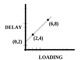
Figure 19 - Typical Delay vs. Loading Relation
1. A line that goes through the coordinates (2,4) and (6,8), or,
2. A line that has a y-intercept of 2 and a slope of 1.
The two-point form is:
(<load1>,<delay1>)(<load2>,<delay2>)In this example, the two-point representation would therefore be:
(2,4)(6,8)which defines a delay whose value is 4 when the loading is 2, and 8 when the loading is 6. Optional whitespace may be placed between the right parenthesis of the first point and the left parenthesis of the second.
The intercept-slope form is:
[<intercept>,<slope>]In this example, the intercept-slope representation would be:
[2,1]Two-point and intercept-slope forms may be used interchangeably.
Constant delays are a special case, with zero slope. For example, a constant delay of 4 could be represented as:
4 or(1,4)(10,4)or[4,0]etc.
Note: if propagation delays depend on input rise and fall times, or if they vary non-linearly with output capacitance, the simple linear delay vs. loading relationship described here would not be applicable. The delay specification formats described in Section 2.7.3.6 Delays Dependent On Input Slew-Rate should be used instead
Global Delays
Global delays are specified in the !DELAY section of the SNL description. Rise and fall delays are independently specifiable. Each global delay characteristic is assigned a unique name that is referenced by individual PART and TYPE statements in the !LOGICAL section. Each global delay definition has the form:
DELAY=<name> RISE=<delay> FALL=<delay>DELAY=<name> CHANGE=<delay>DELAY=del5 RISE=[2,1] FALL=7<typical-delay>;<minimum-delay>;<maximum-delay>where each delay specification is either a two-point or intercept-slope description. For example:
DELAY=del12_8_15 CHANGE=[12,1];8;(0,15)(2,19)The typical delay must be specified. If either the minimum or maximum delay is omitted, it defaults to the typical delay.
Delays are assigned to TYPE and PART outputs with the OUTPUT-DELAY (ODEL) keyword-field, and to busses with the BUS-DELAY (BDEL) key-word-field. The value part of these keyword-fields, which contains the global delay names, is in a one-to-one correspondence with the respective outputs and busses. For example,
P=a2 T=full-adder I=a[2],b[2],c[1] O=s[2],c[2] ODEL=del5,del12_8_15assigns the global delay del5 to output s[2] and del12_8_15 to c[2].
If a signal’s delay is unspecified, the delay defaults to 0. Thus, if the first delay in the above PART statement were omitted:
P=a2 T=full-adder I=a[2],b[2],c[1] O=s[2],c[2] ODEL=,del12_8_15the rise and fall delays of signal s[2] default to 0. Note the placeholder comma preceding the delay name del12_8_15. If this comma were missing, then delay del12_8_15 would be assigned to s[2] and the rise and fall delays of c[2] would default to 0.
As mentioned above, the global delay definitions are specified in the !DELAY section, and are referenced by PART and TYPE statements in the !LOGICAL section:
!DELAY time-units=1e-9
.........
DELAY=del5 RISE=[2,1] FALL=7
DELAY=del12_8_15 CHANGE=[12,1];8;(0,15)(2,19)
.........
.........
.........
!LOGICAL
.........
P=a2 T=full-adder I=a[2],b[2],c[1]
$ O=s[2],c[2] ODEL=del5,del12_8_15
.........
The !LOGICAL section could be in the same network description file as the !DELAY section, or it could be in a different file. Delays defined in a !DELAY section are truly global; that is, available to PART and TYPE statements in all network description files explicitly selected with the GET FILE keyword option or referenced by an !INCLUDE statement. Further-more, the global delay tables can be contained in multiple !DELAY sections, possibly in different files. Regardless of how the delay tables are organized, however, global delay names must be unique. Assigning the same name (e.g., del5) to two different delay characteristics is a fatal error.
Global delays are very convenient when constructing simulation libraries for variants of a particular technology. Here, the functions of the logic cells and loading characteristics are identical, but each variant requires a different set of delay-vs.-loading curves. This is accomplished very simply by creating separate files, each containing a !DELAY section for one variant, and then referencing the appropriate delay table file with the GET FILE option.
Local Delays
Delays may also be assigned locally, within a PART or TYPE statement, without referencing a named global delay. Local delays are unnamed; they are specified directly. This is especially useful for generating SNL descriptions with automated netlisters. The format for defining local delay characteristics is identical to the
ing keywords are OUTPUT-RISE (ORISE), OUTPUT-FALL (OFALL), and OUTPUT-CHANGE (OCHANGE).
For example, assume that a type block named my_type is being defined for a subcircuit that has three input pins, two bidirectional pins, and two outputs pins. Then the TYPE statement:
T=my_type I=a,b,c B=d,e O=f,g BCHANGE=3,4 ORISE=(5,3)(20,4) OFALL=[3,1] OCHANGE=,2assigns:
bus D rise and fall delays of 3
bus E rise and fall delays of 4
output F a rise delay of (5,3)(20,4) and a fall delay of [3,1] output G rise and fall delays of 2.
Delays Dependent On Input Slew-Rate
If input rise and fall times (slew-rates) can significantly affect an element’s propagation delays, or if propagation delays vary non-linearly with output capacitance, use of the simple linear delay vs. loading curve (see Section 2.7.3.3 Linear Delay Curves) may introduce unacceptable errors in computed delays. To handle such technologies, SIMIC supports an alternative, flexible method of describing the (generally non-linear) dependence of propagation delays on output loading and input slew-rates.
Figure 20 illustrates the SIMIC model for slew-rate dependent delays. As shown in Figure 20(a), the actual waveforms are represented by idealized rail-to-rail ramps. In practice, the ramps would be constructed by connecting the points at which the waveform passes through two predefined thresh-olds1 with a straight line, and extending this line to the rails. The rail-to-rail ramp interval, TR, depicts the waveform’s transition time.
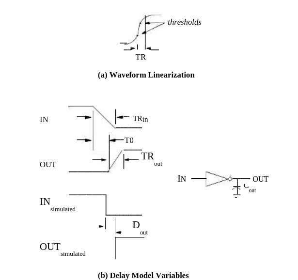
Figure 20 - Slew Rate Delay Model
In order to obtain the required characterization data, you would perform sets of measurements or simulations, linearize the waveforms, and obtain per-cell data on the following three variables (see Figure 20(b)):
TRin – the ramp interval of the cell’s input transition (generated by a driving cell or primary signal),
T0 – the time interval from the start of the input ramp to the start of the output ramp, and
TRout – the ramp interval of the cell’s output.
The measured values should then be scaled to SIMIC time-units.

1. Typical threshold values might be the 30% and 70% points, the 35% and 65% points, etc. In general, the threshold values should not be critical, as long as they are used consistently and are well-selected, i.e., they should bracket the 50% point and be far enough apart to avoid numerical errors, yet close enough to exclude most of the waveform tails.
The delay model assumes that the output measurements, T0 and TRout, are linearly related to the input ramp interval, TRin, and the output loading capacitance, Cout. These relations are described with six parameters; a, b, c, d, e, f:
T0 = a + b×Cout + c×TRin
TRout = d + e×Cout + f×TRin
After obtaining the measurements, you2 would then calculate values for the six parameters to fit the data and generate the corresponding SIMIC delay tables. The format for this delay specification is:
(maxload [a, b, c ,d, e, f])1. Since the operations of obtaining the measurements, linearizing the waveforms, obtaining per-cell values for the three variables, calculating the six coefficients to fit the data, and printing them in the proper format are all regular and repetitive, they can readily be automated, and the amount of actual manual effort need be minimal.
where a, b, c, d, e, and f are the values of the six coefficients, and maxload is the maximum value of Cout for which measurements were taken.
For example:
Delay=Example1 Change=(3e-12 [-6.28, 6e12, .47, 25.3, 1.5e13, .24])If maxload is exceeded in the circuit being simulated, SIMIC will issue a warning.
After reading the circuit description and delay tables, SIMIC computes the values of T0 and TRout for each element output. It then assigns rise and fall delays to each signal (which will execute delayed instantaneous transitions) that extend from the 50% point of the input ramp to the 50% point of the output ramp. For example, referring to Figure 20(b), the square wave-forms illustrate the simulated events corresponding to the waveforms of the actual circuit. The inverter's rise delay would be:
Dout = T0 + 0.5×(TRout - TRin)
In general, the actual dependence of T0 and TRout on loading or input ramp may be non-linear. Thus, SIMIC supports a piecewise linear table format to describe either or both relationships. To describe a non-linear loading relationship, you specify the coefficients within the regions of the curve, and the breakpoints from one region to the next in the Ctable format:
(maxload1 [a1 ,b1 ,c1, d1, e1, f1] maxload2 [a2, b2, c2, d2, e2, f2] ...)where maxload1, maxload2, etc. are the upper breakpoints for the linear regions, and a1-f1, a2-f2, etc. are the lists of six coefficients that apply for the first region, the second region, etc. For example:
Delay=Example2 Change=($
             1e-13 [.4, -2.5e-12, .6, 3.1, 4.3e13, -.3] $
             3e-13 [.6, -2.3e-12, .5, 3.6, 4.6e13, -.4] $
           )
In this example, the first set of coefficients are used if the loading is less than or equal to 1e-13, and the second set of coefficients are used if the loading is above 1e-13 and less than or equal to 3e-13. Because this is the last region described, it will also be used for loadings above 3e-13, but a warning will be issued.
Note that as a special case, the Ctable format can also be used to handle non-linear delay vs. loading characteristics for technologies in which output loading is the only significant factor affecting propagation delays. This is accomplished by setting the c, d, e, and f coefficients (those associated with input slew-rates) to 0. Essentially, each entry specifies the intercept and slope of the piecewise linear approximation for a range of capacitive loads. For example:
Delay=Example2 Change=($
             1e-13 [.4, -2.5e-12, 0, 0, 0, 0] $
             3e-13 [.6, -2.3e-12, 0, 0, 0, 0] $
           )>
To describe non-linear input ramp relationships in a piecewise linear fashion, use the Rtable format:
(maxramp1 Ctable1 maxramp2 Ctable2 ...)where maxramp1, maxramp2, etc. are the upper breakpoints for the linear regions, and Ctable1, Ctable2, etc. are in the Ctable format described above. The following is an example of a segmented input slew table:
Delay= N1P1 $
    Rise= ( 5 (7e-13 $
                 [0.4,-2.5e12,0.6,3.2,4.3e13,-0.4])$
           10 (3e-12 $
                 [0.6,-2.3e12,0.5,3.6,4.6e13,-0.4])$
          250 (3e-12 $
                 [8.9,-4.8e12,0.7,-4.8,4.6e13,0.1]))$
    Fall= ( 5 (7e-13 $
                 [0.2,-1.4e12,0.6,2.5,2.8e13,-0.4])$
           10 (3e-12 $
                 [0.03,-9.8e11,0.6,3.3,2.9e13,-0.6])$
          100 (3e-12 $
                 [1.1,-1.1e12,0.6,9.4,2.5e13,0.06])$
          250 (3e-12 $
                 [-6.3,6e12,0.5,25.3,1.5e13,0.2]))
Note: like the linear two-point and intercept-slope delay forms, the Ctable and Rtable forms can be used in local as well as global delay specifications.
Since the cells driven by the primary inputs must also be assigned delays, primary inputs should be assigned a reasonable “default” ramp interval. This is accomplished with RAMP keyword in the !DELAY section. For example:
!DELAY RAMP=5assigns the ramp interval TR = 5 time-units at each of the primary signals. The specified ramp interval is also assigned at all internal signals whose delay tables are not in Rtable format to allow intermixing of input slew-rate dependent and input slew-rate independent cells in the same design with reasonable results. The RAMP keyword may also be specified on a separate line within the !DELAY section.
Specifying Pin Loading
Loading can be specified for all pins of a TYPE statement and all pins of an instantiated component in a PART statement. A load value can also be specified for each signal, typically representing wiring capacitance. Load values are specified as fixed-point or floating-point numbers. If no loading is specified for a signal or a pin, then the loading value is defaulted to 0.
Like delays, the general format for specifying loading is a three-tuple of values—typical, minimum, and maximum—separated by semicolons.
The keywords for specifying pin loads in PART and TYPE statements are BUS-LOADS (BLOD), INPUT-LOADS (ILOD), and OUTPUT-LOADS (OLOD) for bus, input, and output pins, respectively. The specified values are in a one-to-one correspondence with the respective signals. For example, adding loading to the above TYPE statement for my_type:
T=my_type I=a,b,c B=d,e O=f,g BCHANGE=3,4
            ORISE=(5,3)(20,4) OFALL=[3,1] OCHANGE=,2 ILOD=1,,3 $
BLOD=5;4;6,7.89 OLOD=10,11input pin A a load of 1
input pin B a load of 0 (since no loading is specified)
input pin C a load of 3
bus pin D typical,minimum,maximum loading of 5;4;6
bus pin E a load of 7.89
output pin F a load of 10
output G a load of 11.
Nets are assigned loading by instantiating the built-in LOAD element:
P=<name> T=load O=<net-name> OLOD=<value>or
P=<net-name> T=load OLOD=<value>where:
- <net-name> is the hierarchical name of the net
- <value> is the load value assigned to the net.
In the first form, with the OUTPUT keyword-field explicitly specified, the assigned part name,
As an example of the second form, the statement:
PART=a.b.c TYPE=load OLOD=3;2;5assigns typical,minimum,maximum loading of 3,2,5, respectively, to the signal named a.b.c.
Resultant Delays
When a load-dependent driver delay is specified, either by reference to a global delay or by a local delay, the SIMIC compiler totals all loading associated with the driven net to obtain the resultant delay from the specified delay vs. loading characteristic. Calculations are performed in floating point, and the results rounded to the nearest integer.
For example, in the circuit shown in Figure 21 the total loading on the net named signal is (1.1 + 2.6 + 2.5 + 3.4 =) 9.6. Thus, the AND gate’s rise delay is 24 (5 + 2×9.6 = 24.2 rounded down), and its fall delay is 13 (3 + 1×9.6 = 12.6 rounded up).
If the result after interpolation is negative, SIMIC sets the delay to 0.

P=driver t=and i=a,b o=signal orise=[5,2] ofall=[3,1] olod=1.1
p=load1 t=inv i=signal ilod=2.6
p=load2 t=inv i=signal ilod=2.5
p=signal t=load olod=3.4
Figure 21 - Delay Computation Example
Delays At Paralleled Elements
Drivers are sometimes paralleled to decrease rise and fall delays for heavily-loaded busses. Usually, the drivers are either identical or at least close in their drive capabilities. The SIMIC compiler considers elements paralleled when (1) their outputs are tied together, (2) they are all the same type, which must be one of the following built-in primitives: INV, AND, NAND, OR, NOR, BTGRN, BTGRP, UTGRN, or UTGRP, and (3) they have the same inputs (though not necessarily in the same order). When these criteria are met, SIMIC replaces the paralleled elements with a single element whose delay characteristic has:
1. a y-intercept that is the minimum y-intercept of all the paralleled elements, and
2. a slope obtained by treating the slope of each element's delay vs. loading characteristic as a resistance and computing the equivalent resistance of the parallel combination
The rise and fall delay constructions are performed independently. Figure 22 illustrates this replacement.
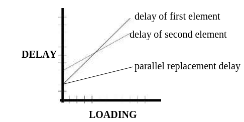
Figure 22 - Illustration of Parallel Element Delay Reduction
Modifying Delays At Run Time
The SET command can be used to modify delays at run time. This is useful for circuit debugging and experimentation. The options that can be specified are:
1. <n> - set delay to the specified value,
2. +<p>% or −<p>% - increase or decrease delay by the specified percent-age, <p> (an integer). (Note: the + sign is optional)
The RISE, FALL, and CHANGE keywords are used to specify that rise delays, fall delays, or both, respectively, be modified in the requested manner. The LIST keyword specifies which signals should be affected. For example,
SET RISE=30 LIST=a,b,csets the rise delay of the three signals to 30, while
SET CHANGE=-10% LIST:reduces all delays by 10% (note that specification of a percentage less than, or equal to, -100% will set the affected delays to 0).
Section 2.6.12 Modifying Delay Values contains a more complete description of interactive delay modification.
Decays
By default, SIMIC instantaneously sets a floating net to the Z state, which represents an unknown value at floating strength. Decay times can be set to non-zero values on a per-node basis either in the circuit’s SNL description of by using the SET DECAY run command (see Section 2.7.4.2 Modifying Decays At Run Time).
When a node has a non-zero decay time, its value instantaneously changes to C, representing logic 1 at floating strength, if it was previously a driven 1, or to D, representing logic 0 at floating strength, if it was previously a driven 0. The node will remain at these values until it decays to Z (or it is driven again).
Specifying Decays In SNL
Decay characteristics are specified in PART or TYPE statement with the BUS-DECAY (BDEC) keyword-field for busses or the OUTPUT-DECAY (ODEC) keyword-field for outputs. The specified values for these key-words have a one-to-one correspondence with the busses and outputs, respectively. The decay values that can be specified are:
1. a positive number specifying the decay time
2. the name of a global delay
3. the reserved word INFINITE, or any prefix of this word.
The first and third options are self-explanatory. The second option, specifying a global delay, allows the decay time to depend on loading (capacitance). Since delay characteristics specify two delays, rise and fall, the node’s decay time is taken as the average value of the two delays for the given node capacitance. Generally, it is easiest to represent load-dependent decays by creating special global delays that contain the CHANGE keyword-field.
For example, the TPADN, a built-in primitive, is a tristating element with two inputs, EN (enable) and D (data). When EN is logical-1, the output is equal to the data input, and when EN is logical-0, the output tristates. Given the PART statement:
p=tri t=tpadn i=enable,data5 o=out5 odec=del83suppose that, for the capacitance at the net named out5, the rise and fall delays for the delay characteristic del83 are 90 and 110, respectively, Then the decay time for this net will be their average value, 100.
Note: if different decay times are specified for a signal that has multiple drivers (wire-tie), then the signal’s decay will be the minimum value specified for any of its drivers.
Modifying Decays At Run Time
The SET DECAY command can be used to modify decays at run time. The DECAY keyword supports the same three options as the SET command’s delay modification keywords, plus a fourth option, setting infinite decay:
1. <n> - set decay to the specified value, <n> (an integer)
2. +<p>% or −<p>% - increase or decrease decay by the specified percent-age, <p> (an integer). (Note: the + sign is optional)
3. * - restore original decay from SNL description
4. INFINITE - set decay to infinite (any prefix of this word is valid)
The LIST keyword specifies the signals to be affected by the selected option. For example:
SET DECAY=infinite LIST=a,bsets the decays of the two signals to infinite.
Input High Impedance Default
By default, the value Z, unknown value at floating strength, is treated as an X at (unidirectional) element inputs that are not strength-sensitive. (Of course, a signal’s strength may be very important at bus pins, where the signal may be wire-tied. and flow may be bidirectional.)
This default is applicable to many modern technologies. For example if a CMOS inverter’s input is floating, its output value will be uncertain. How-ever, it is not correct for all technologies. In current-mode logic, a floating signal may be equivalent to 0. In the old DTL technology, a floating signal is equivalent to 1 at an AND gate input, and to 0 at an OR gate input.
If the default is inappropriate, the logical equivalent of Z may be explicitly specified in PART and TYPE statements, on a per-input basis, using the INPUT-HIZ (IHIZ) keyword-field. For example, the PART statement:
part=d type=and i=a,b,c ihiz=1,0specifies that a floating unknown value should be treated as logical-1 at input a, and as logical-0 at input b. Since no IHIZ value is specified for input c, a floating unknown at this input will be treated as X.
Verifying Timing Tolerances
When simulation is performed to verify logical correctness and completeness, timing considerations are deferred. At this time, the effects transient input states and narrow margins between events are ignored. However, in the final phases of design verification, these situations must be detected and corrected to eliminate potential timing problems.
Functional Timing Checks
Timing checks are supported for the DNL and DPL (DL) latch and the DNCF, DPCF (DCF), JKNCF (JKCF), JKPCF, TNCF (TCF), and TPCF edge-triggered flip-flops. These checks can be specified within a TIMING-CHECKS block in any PART statement instantiating these built-in primitives.
In the following description, the active clock edge is the clock transition that causes the latch or flip-flop output to change state. This edge is the rising clock transition for the DPL (DL), DPCF (DCF), JKPCF, and TPCF primitives, and the falling clock transition for the DNL, DNCF, JKNCF (JKCF), and TNCF (TCF) primitives.
The supported timing checks are:
1. SETUP – this check specifies the minimum duration that an input must be stable prior to an active clock edge:
- DNL, DPL, DNCF, DPCF – setup from D (SETUP.D)
- JKNCF, JKPCF – setup from J (SETUP.J) and setup from K (SETUP.K)
- Additionally, all eight primitives support setup from reset (SETUP.NR), and setup from set (SETUP.NS). These setup times represent the minimum duration that the reset (set) must be inactive to reliably set (reset) the memory element via clock
2. HOLD – this check specifies the minimum duration that an input must be stable after an active clock edge:
- DNL, DPL, DNCF, DPCF – hold to D (HOLD.D)
- JKNCF, JKPCF – hold to J (HOLD.J) and hold to K (HOLD.K)
- Additionally, all eight primitives support hold to reset (HOLD.NR), and hold to set (HOLD.NS)
3. PULSE-WIDTHS – this check specifies the minimum width of a pulse on the set, reset, or clock lines. All eight primitives support: pulse-width reset (PW.NR), pulse-width set (PW.NS), and high and low pulse-width clock (PW.C.H and PW.C.L respectively).
The setup and hold checks for the asynchronous, active-low, set and reset inputs of all eight primitives are associated with the time duration between the rising (trailing) edge of pulses on these inputs and the active clock edge.
Unspecified timing checks default to 0 (disabled).
The syntax of a TIMING-CHECKS block is:
TIMING-CHECKS=begin; <spec>; …;<spec>; end;where <spec> is a timing specification of the form <timing-check> = <limit>
Referencing a timing check by itself, without a qualifying pin name or clock level—SETUP, HOLD, PW—specifies all checks of that type. For example, in a TIMING-CHECKS block for a JKCF instance, SETUP specifies all setup checks; SETUP.J, SETUP.K., SETUP.NR, and SETUP.NS. Values specified for qualified timing checks supercede those specified for unqualified checks.
As an example, the timing block:
part=FF1 type=DCF i=reset,set,clk,data o=q1 $
    timing-checks= $
    BEGIN; $
    SETUP = 5; $
    HOLD.D = 10; $
    HOLD = 5; $
    PW = 4; $
    PW.C.L = 3; $
    END;
specifies:
1. All setups are 5 units.
2. All holds are 5 units, except hold from D which is 10.
3. All pulse-widths are 4, except clock-low pulse-width is 3.
Delay vs. loading curves, as well as MINIMUM, TYPICAL, and MAXIMUM delay sets can be used for specifying <limit>. If delay curves are used, then the loading on the part’s output is used to determine the timing check value. The syntax is identical to specifying local delays. For example:
timing-checks= $
    BEGIN; $
    SETUP = 25;20; $=maximum delay same as typical
    HOLD = [4,2];[3,1];[5,3]; $
    PW = (5,1)(7,3);4;[9,3]; $
    END;
Controlling Spike Propagation
Section Combinational Timing Hazards describes the spike hazard, a timing problem characterized by a sequence of changes at an element’s inputs such that an element output begins responding to the first input state, but before its response time elapses, a second input change occurs, causing the output to return to its original value. This situation is illustrated in Figure 23 for a two-input AND gate.
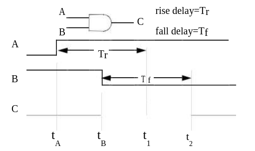
Figure 23 - Spike Hazard At An AND Gate
In this figure, the rise at signal A would normally cause output C to rise at time
t1 = tA + Tr
However, at time tB < t1, signal B executes a transition to 0, which forces signal C to be 0 at, or before, time
t2 = tB + Tf.
What value or values should signal C be assigned in the interval between tB and t2?
Since propagation delays are inertial, i.e., associated with charging and dis-charging node capacitance, and since, by assumption, the time required to charge signal C to the logic-1 threshold is Tr, one possible answer to this question is to maintain C at a constant 0, since the peak voltage level it reaches at time tB must be less than this threshold. This model, which ignores (filters out) the effects of transient input states whose duration is less than the output’s response time, is called inertial filtering.
Alternatively, since simulation is usually performed to predict the circuit’s operation in the real world, and since actual input arrival times, gate delays, and wiring delays will almost certainly differ from simulated values (the operation of circuits from separate production lots will also differ), it is very possible that an output pulse that almost happened during simulation will actually happen on some manufactured chips. Thus, another possible
answer to the above question, based on a conservative approach, is to set the value of signal C to X within this interval, since actual operation may be indeterminate at the time of simulation. This model, which creates an X-pulse when a spike hazard is detected, and propagates this pulse to all fanouts, is called spike propagation.
SNL supports flexible per-node control on the degree of pessimism introduced into spike propagation. The SIMIC XPROPAGATE run command provides the same control at run time (see Section 2.6.18 Enabling And Disabling X-Propagation).
Two parameters may be specified in any PART or TYPE statement to control spike propagation at each output:
1. filter – specifies a transient width threshold. Spike-producing transient input states that are narrower than this threshold will be inertially filtered, while transients at least as wide as the threshold will be propagated as X-pulses, if possible (the transient may still be filtered because of large differences between rise and fall delays; see below).
2. liberal – controls when to start the X-pulse. An X-pulse always ends at the time that the affected signal in guaranteed to have reached its known final value.
The filter threshold is expressed as percentage of the output’s response time. Thus, in the above example, if this threshold is 10%, then the spike will be inertially filtered if the difference in arrival times of the events at A and B, t B – tA, is less than 0.1×Tr. This value is specified as an integer between 0 and 100, inclusive, optionally followed by a percent (%) sign.
The value filter=0 introduces the greatest pessimism, since any input transient is at least as wide as this threshold. The value filter=100 introduces no pessimism, since all input transients are inertially filtered (this threshold corresponds to an input whose duration is the response time; but this is not a spike situation since the output has exactly enough time to respond).
The liberal value linearly controls the start of the X-pulse between the extremes of (a) the time of the input event causing the spike and (b) the time that the output would have responded to the first event. In the above example, these extremes are tB and t1. Adopting this notation to describe the general case, the X-pulse starts at time
tstart = tB +
where
The value liberal=0 introduces the greatest pessimism, since it starts the X-pulse at tB, the time that the spike hazard is detected. The value
liberal=100 introduces the least pessimism, since it starts the X-pulse at t1.
Note that when an output’s rise and fall delays differ sufficiently, its response to the second input event can be earlier than its response to the first event. Using the notation of the above example, t2 may be earlier than t1 if Tf is sufficiently small. Since the X-pulse always ends at t 2, and since it is
possible to specify a liberal values that bring tstart close to t1, it is there-fore possible to specify a starting time for the X-pulse that is later than its
ending time. If this situation occurs, the X-pulse is not generated, and the transient input state is effectively inertially filtered.
The SNL keywords that specify the filter parameter are BUS-FILTER (BFILTER) for busses and OUTPUT-FILTER (OFILTER) for outputs. Similarly, the SNL keywords that specify the liberal parameter are BUS-LIBERAL (BLIBERAL) for busses and OUTPUT-LIBERAL (OLIBERAL) for outputs.
Unspecified values for any of these keyword options are defaulted to 0, the most pessimistic settings. To globally disable spike propagation when verifying logical correctness rather than timing, use the
NO XPROPAGATE SPIKE:
command (see Enabling And Disabling X-Propagation in Circuit Troubleshooting).
As an example, the PART statement
p=p15 t=xyz i=a,b,c o=d,e,f $ odel=dela,delb,delc ofilter=10%,,50 $ oliberal=30,20%
assigns:
output D a filter value of 10% and a liberal value of 30% output E a filter value of 0 and a liberal value of 20% output F a filter value of 50% and a liberal value of 0
Wire-Ties
Wire-ties are created by assigning different element outputs or busses the same signal name. Figure 24 illustrates this situation for the outputs of two TPADN primitives having the identical output signal, sig. Wire-ties can also be created dynamically, when two differently-named signals are connected through an ON ideal switch (BTGN or BTGP).
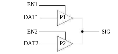
Figure 24 - Sample Wire-Tie
p=p1 t=tpadn i=en1,dat1 o=sig odel=del1 $ odecay=dec1
p=p2 t=tpadn i=en2,dat2 o=sig odel=del2 $ odecay=dec2
Figure 24 - Sample Wire-Tie
Wire-Tie Dominance
If, in Figure 24, only one of the TPADN elements drives sig (the other being disabled with its enable input at logical-0), or if both elements drive the same level, then the value at sig is well-defined. If the elements simultaneously drive different values, then a conflict exists, and the resulting value at sig depends on the specified wire-tie characteristics. SIMIC sup-ports three types of wire-ties:
1. Wired-AND (0-dominance) – if any of the strongest components connected to the wire-tie is driving a logical-0, then the signal’s value is 0
2. Wired-OR (1-dominance) – if any of the strongest components connected to the wire-tie is driving a logical-1, then the signal’s value is 1.
3. CONFLICT (X-dominance) – if either (a) the state of at least one of the strongest drivers connected to the wire-tie is unknown, or (b) one or more of the strongest drivers is driving logical-0, while one or more of the remaining strongest drivers is simultaneously driving logical-1, then the signal’s value is undefined (set to X).
A wire-tie’s dominance can be specified in a PART or TYPE statement with the BUS-DOMINANCE (BDOM) keyword-field for busses or the OUTPUT-DOMINANCE (ODOM) keyword-field for outputs. These keywords associate in a one-to-one correspondence with the PART or TYPE statement’s busses and outputs, respectively. The values expected for these keywords are the
dominance categories 0, 1, or X.
For example, assume that a part has three outputs, each tied to other signals (but not to each other). If the wire-tie associated with the first output functions as a wired-AND, the wire-tie associated with the second output functions as a CONFLICT tie, and the wire-tie associated with the third output functions as a wired-OR, then ODOM=0,,1 should be specified in the PART statement.
If the dominance is unspecified, the default wire-tie type is CONFLICT (ODOM=X). Thus, wire-tie dominance only requires specification at wire-tied signals whose mutual interaction functions as a wired-AND or wired-OR.
A wire-tie’s dominance can be specified in any PART or TYPE statement associated with the common signal. If specified for more than one driver, the specifications must be identical.
For example, in the circuit of Figure 24, neither PART statement specifies a dominance for signal sig, so by default, the wire-tie is X-dominant. Placing an output dominance specification in either PART statement, or in both, specifies the wire-tie’s dominance, even if other drivers are connected to sig. If placed in multiple statements, all dominance specifications must be identical.
Sometimes, especially when functions are described at the switch level, a CONFLICT tie can generate a known result when an uncertain value would be more appropriate. This can occur during fault simulation, when a fault introduces a conflict that should not happen in the non-faulted circuit, or during circuit debugging, when a design error causes pullup and pulldown paths to conduct simultaneously.
For example, consider a CMOS inverter, where the P-device has a 5% greater ON-resistance than the N-device. If a fault puts the P and N devices in conflict, then the inverter’s output voltage would be approximately 0.49×VDD, not a logical-0 or logical-1. However since the N-device has a smaller ON-resistance, a CONFLICT tie would resolve the result to be a logical-0., and the fault might erroneously be classified as detected. Perhaps it would be more appropriate if the output value were unknown for this case.
The ODOM keyword also supports specification of logical-0 and logical-1 thresholds for wire-tie conflicts. Thresholds represent percentages of the full output voltage swing; they are specified as a pair of integers between 0 and 100 inclusive, enclosed within square brackets:
ODOM = [T0,T1]
where T0 is the logical-0 threshold, T1 is the logical-1 threshold, and T0 < T1.
When thresholds have been specified with the ODOM keyword, SIMIC treats the series depths of the ON switches as equivalent resistances and calculates the “voltage divider” ratio:
Sn / (Sn + Sp)
where Sn is the series depth of the pulldown path and Sp is the series depth of the pullup path. It then resolves the wire-tie conflict as follows::
- If this ratio is less than T0, or equal to T0 and T0 < T1, the output is set to logical-0.
- If this ratio is greater than T1, or equal to T1 and T0 < T1, the output is set to logical-1.
- Otherwise the output is set to X.
If the dominance of the CMOS inverter output in the above example had been assigned, say, the value ODOM=[30,70], then since 0.3 < 0.49 < 0.7, the inverter output in the faulted circuit would have been assigned the value X. The output value would only have been resolved as logical-0 if the series depth ratio were 0.3 or less. This would require the P device’s ON resistance to be at least 2.33 times the N device’s ON resistance:
Sn / (Sn + Sp) > 0.3 or 0.7×Sn < 0.3×Sp or 2.33×Sn < Sp
As special cases, the threshold specification [0,0] is equivalent to a wired-AND, [100,100] is equivalent to a wired-OR, and [50,50] is equivalent to a CONFLICT tie.
Specifying Drive Strength
Most wire-tied configurations are designed to have at most one active driver at any one time (e.g., address and data lines between a CPU, ROM, and RAM). Sometimes, however, correct operation requires that a strong driver overpower a weaker one. For these situations, it is necessary to incorporate drive strength into driver models.
Drive strength can be specified in any PART or TYPE statement. This value can be one of the following reserved words:
POWER, DRIVING, RESISTIVE, FLOATING.
Any prefix of these words is valid.
High (pullup) and low (pulldown) drive strengths may be specified independently, or simultaneously if identical. The associated keywords are:
BUS-DRIVE (BDRIVE) – high and low drive strength for busses BUS-LDRIVE (BLDRIVE) – low drive strength for busses BUS-HDRIVE (BHDRiVE) – high drive strength for busses OUTPUT-DRIVE (ODRIVE) – high and low drive strength for
outputs
OUTPUT-LDRIVE (OLDRIVE) – low drive strength for outputs OUTPUT-HDRIVE (OHDRiVE) – high drive strength for outputs
If a signal’s high or low drive strength is unspecified, the default strength is DRIVING.
For example, the PART statement:
P=p22 T=xyz I=a,b,c B=d,e O=f,g BHDRIVE=,res BLDRIVE=fl,pow ODRIVE=pow,resassigns the following drive strengths:
bus D – high-drive=DRIVING, low-drive=FLOATING
bus E – high-drive=RESISTIVE, low-drive=POWER
output F – high-drive=low-drive=POWER
output G – high-drive=low-drive=RESISTIVE
Additionally, the BTGRN and BTGRP resistive bidirectional switches and the UTGRN and UTGRP resistive unidirectional switches can be assigned depths with the SERIES-DEPTH (SDEPTH) keyword-field. (The subsection Depths And Strengths in Circuit Troubleshooting describes the correspondence between series depths and drive strengths.) The series depth value may be an integer between 1 and 32,767 inclusive. If unspecified, the default series-depth is 1.
Figure 25 illustrates a sample circuit that requires proper drive strength assignments in order to model its operation. The inverter loop represents a single memory cell inside a RAM. The bit line connects to all cells associated with a particular memory bit through series transistors, only one of which is ON at any time. The write amplifier, w, drives the bit line at POWER strength. When this value propagates through the series transistor, with a series-depth of 1, its strength is reduced to DRIVING. This is strong enough to overcome the RESISTIVE strength of inverter i2, so the value of d_in is written into the memory cell.
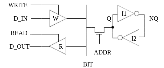
p=w t=tpadn i=write,d_in o=bit odrive=pow
p=r t=tpend i=read,bit, o=d_out
p=x t=btgrn  i=addr  b=bit,q  sdepth=1
p=i1 t=inv i=q o=nq odrive=resistive
p=i2 t=inv i=nq o=q
Figure 25 - Memory Cell Read/Write Circuit
Hierarchical Precedence of Electrical Attributes
SNL maintains a top-down hierarchical precedence for electrical attributes (delay, loading, decay, drive strength, IHIZ default) as well as for signal names. Electrical attributes specified at a higher level of the hierarchy over-ride, or take precedence over, corresponding specifications at a lower level. Thus, any attribute specified in a PART statement overrides the corresponding value specified in the instantiated part’s TYPE statement, which, in turn, overrides the corresponding attribute value specified in its constituent PART statements.
The following example illustrates hierarchical precedence. It defines a type block, hier_demo, that contains two xor macro instances (the XOR is a gate-level implementation of a 2-input exclusive-or). The sequential column numbers at the left are “source line” designations, that are referenced below, and are not part of the SNL description:
1. !delay
2. delay=del1 rise=3
3. delay=del2 change=1
4. !logical
5. type=hier_demo i=a,b,c,d o=e,f ilod=,,,10 odel=,del1
6. p=xor1 t=xor i=a,b o=e ilod=7 olod=3
7. p=xor2 t=xor i=c,d o=f ohdrive=res odel=del2
8. type=xor i=x,y o=z ilod=,8 olod=4
9. p=n1 t=nand i=x,y ilod=1,1
10. p=n2 t=or i=x,y ilod=2,2
11. p=z t=and i=n1,n2 orise=5 ofall=6
The electrical attributes at the pins of an isolated xor type block are:
| pin | loading | source line |
|---|---|---|
| x | 3 | 9,10 (sum of pin loads) |
| y | 8 | 8 (overrides 9,10) |
| z | 4 | 8 |
| pin | delay | source line |
|---|---|---|
| z | rise=5, fall=6 | 11 |
The electrical attributes at the pins of the hier_demo type block are:
| pin | loading | source line |
|---|---|---|
| a | 7 | 6 (overrides 9,10) |
| b | 8 | 8 (overrides 9,10) |
| c | 3 | 9,10 |
| d | 10 | 5 (overrides 8 which overrides 9,10) |
| e | 3 | 6 (overrides 8) |
| f | 4 | 8 |
| pin | delay | source line |
|---|---|---|
| e | rise=5 fall=6 | 11 |
| f | del1 | 5 (overrides 7 which overrides 11) |
Note that the delay at output f is del1, as specified in the type statement of hier_demo. This completely overrides the ODEL=del2 specification in the PART statement for xor2, even though del1 has no fall delay specified. This is because the missing fall delay specification in del1 causes an implicit assignment of 0 for this delay, and the rise/fall delay pair of del1 (3/0) overrides the rise/fall delay pair of del2 (1/1).
Unused Bus and Output Pins
If a type block has a fixed number of pins, as defined in its TYPE statement, then it is an error if the number of inputs, outputs, or busses specified in an instantiating PART statement does not match those in the TYPE statement. Sometimes, however, output or bus pins of instantiated types are not used.
In this case, the UNUSED reserved word should be specified as the “connection” for these pins; it is self-documenting, and it informs SIMIC that no error was made specifying connectivity.
For example, Figure 26 illustrates a macro, DFF, containing a DCF and in inverter to make the q output available. Also shown are two part statements (within another type block) that instantiate this macro. The second instance does not use the q output of the macro. Note that because of the UNUSED entry, the q signal of instance ff2 has no user-assigned name. It can still, however, be examined during simulation, if necessary. An UNUSED pin is “pushed into” the macro, for this macro instance. Thus, the q signal in ff2 can be referenced as ff2.q.
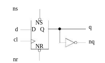
type=dff i=nr,ns,cl,d o=q,nq p=q
t=dcf i=nr,ns,cl,d o=q p=nq
t=inv i=q
....................................
c= these part statements are in a different type block
p=ff1 t=dff i=nr1,ns1,cl1,d1 o=q1,nq1 p=ff2
t=dff i=nr2,ns2,cl2,d2 o=unused,nq2
Figure 26 - Example of Unused Instance Pin
Specifying Level of Abstraction
Sometimes, when a subcircuit requires optimization or when multiple designs of the subcircuit are being investigated, multiple descriptions of the subcircuit will be created and tested. It is convenient to assign all variants the same type name, since it may be instantiated many times; using different names would require editing the netlist each time another variant is tested. Any component instantiated in a PART statement will have one of the fol-lowing levels of abstraction:
MACRO, BOOLEAN, BEHAVIORAL, PRIMITIVE.It is an error to assign the same type name to multiple type blocks at the same level of abstraction. For example, every macro’s type block must have a unique name. If multiple type blocks at the same level of abstraction have the same name, SIMIC will accept the first definition found, and issue a warning message that multiple type blocks have identical names. The solution is to place the variant definitions in separate files, and select the appropriate file with the GET FILE keyword option.
In contrast, identically-named variants defined at different levels of abstraction can be placed in the same file. For example, one definition of a full-adder could be a macro, and another could be, say, a BOOLEAN type. The COMPOSITION keyword-field is used to specify which model (level of abstraction) is referenced by each instantiating PART statement.
If the COMPOSITION keyword is not specified, the SIMIC compiler searches for definitions in the order listed above. Thus, in the above situation, SIMIC would always instantiate the MACRO full-adder definition. To instantiate the BOOLEAN definition:
p=fad t=full-adder i=a1,b1,c1 o=s1,co1 composition=booleanSIMIC also issues a warning message when type blocks at different levels of abstraction have the same name. For example (although not good practice), it is possible to define a MACRO or BOOLEAN having the same name as a SIMIC primitive, which would always be instantiated instead of the primitive unless the PART statement contains COMPOSITION=PRIMITIVE. This could lead to considerable confusion without the message.
Although unrelated, the COMPOSITION keyword serves another function. It is an error to define a type block containing only a TYPE statement unless it is a BOOLEAN type block. In this case, the TYPE statement would contain a BOOLEAN equation block identifying it as such. Sometimes, how-ever, when experimentation is necessary, it may be desirable to omit the equations from the SNL description and specify them at run time, via the CLAMP command. In this case the keyword-field COMPOSITION=BOOLEAN should be placed in the TYPE statement to identify it as a BOOLEAN type in place of the missing equations.
Physical Size Metric
SIMIC supports three metrics that can provide assistance in obtaining estimates of the main type’s physical size. These metrics are:
- PADS – the number of physical pads for the cell
- TRANSISTORS (TRANS) – the number of transistors in a cell
- WIDTH (W) – the width of a cell
These keyword-fields may be placed in any PART or TYPE statement.
Their associated values are integers:
PADS=<integer>
TRANS=<integer>
WIDTH=<integer>
SIMIC makes no use of these numbers other than to total them during compilation, whenever a PART or TYPE statement containing the metrics is encountered, and report their respective sums.
In a standard cell methodology, the metrics should be placed in the TYPE statement for each cell, and the instantiating PART statements should not contain them. The resulting sums reported by SIMIC would then represent the total physical contributions of all instantiated cells.
In a custom design methodology, the cell TYPE statements might contain metrics for the smallest possible cell, and instantiating PART statements might contain the differences between these values and the actual instance values.
For example, if the TYPE statement of the full-adder in Figure 15(a)
is changed to include size metrics:
type=full-adder i=ia,ib,c-in o=sum,c-out trans=26 width=50the messages SIMIC issues in response to the GET command for compiling the four-bit adder would be:
Main Get Network : FOUR-BIT
GET completed, Circuit totals: Parts = 21; Signals = 32 Inputs = 9; Busses = 0; Outputs = 6
Physical Totals:
    Width = 200
    Transistors = 104